Sorry your browser is not supported!

You are using an outdated browser that does not support modern web technologies, in order to use this site please update to a new browser.

Browsers supported include Chrome, FireFox, Safari, Opera, Internet Explorer 10+ or Microsoft Edge.

Geek Culture / Can't Get An And Gate IC To Work Properly

Author
Message
Dark Java Dude 64
Community Leader
14
Years of Service
User Offline
Joined: 21st Sep 2010
Location: Neither here nor there nor anywhere
Posted: 14th Feb 2012 06:50 Edited at: 14th Feb 2012 06:52
Hey everyone. I recently tried plugging my CMOS AND gate chip into a PCB i have assembled and it didnt work. So, i took the IC and put it into a breadboard. All of this time i have been using a lot of anti static precautionary measurements. I had VCC connected to 3.8 or so volts positive, and ground to negative. The datasheet specifies 2 to 6 volts for power supply. I connected a multimeter to the output and got around 3.5 volts, even though neither of the inputs were connected to high.

Edit: Mid writing this post i realized what i was doing, so though the prob is likely solved ill explain the remedy anyway:

The wires, after being touched to say, a logical high, remained high until they were placed on the logical low, even without touching the logical high terminal. So, i was suffering from the capacitance of the wires!

Darn it, i was going to put the comet to work to answer this but i guess hes off the hook!

Copyrightz © 2012 dbd79
HowDo
22
Years of Service
User Offline
Joined: 28th Nov 2002
Location: United Kingdom
Posted: 14th Feb 2012 10:18
I think you found out that when both are high the output works.

Dark Physics makes any hot drink go cold.
TheComet
17
Years of Service
User Offline
Joined: 18th Oct 2007
Location: I`m under ur bridge eating ur goatz.
Posted: 14th Feb 2012 13:09 Edited at: 14th Feb 2012 13:09
Quote: "Darn it, i was going to put the comet to work to answer this but i guess hes off the hook!"


Still doesn't mean I can't explain in-depth of what happened so everyone understands

Although you haven't really supplied enough information, I think I know what your problem is. I'll start with the input problem.

The Input

CMOS input stages in logic ICs almost always look something like one of the following:


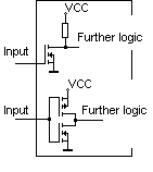
So what happens when we leave the input wire open (hanging in the air)? Most of the time you will actually destroy the IC because it will begin to conduct a high amount of current due to unclean signals. You mentioned this at the end when you touched the input with your finger. Because the GATE of the CMOSFET has a capacitance, you charged it just by touching it and it started to conduct electricity. So here's the rule.

NEVER EVER EVER LEAVE CMOS IC INPUTS OPEN

How do we fix it?

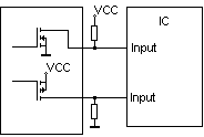
The clean way of attaching an input is to use a pull-up or pull-down resistor. These resistors are always 10k. Here's an example:


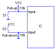
Pull-ups and Pull-downs make sure that when you don't connect anything to the IC, the input will have a defined state (it won't be "open"), and you don't risk destroying the IC due to overvoltage through static discharge. You can of course replace the switches with a transistor, or even another IC:


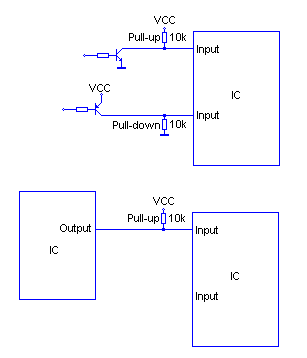
I'll explain the "connecting another IC" a little deeper, as it requires some additional knowledge for it to work properly.

What do I do with the input wires I don't need?

This:


All inputs on a CMOS IC must have a defined state, or it's possible they'll turn themselves into a small nuke cloud.

The Output

So now that we know how inputs work, let's look at the output stage of a CMOS. There are two common ways of making outputs (there are other ways, but I won't discuss them here). There's the push-pull configuration (sometimes referred to as "totem-pole configuration"):


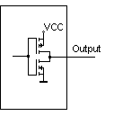
And then there's the Open Drain configuration:


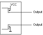
If the output is a push-pull, you don't need any pull-up or pull-down resistors. If you have an open drain output, you need the resistors to pull in the opposite direction.


Hope that clarifies a few things for you

TheComet

Attachments

Login to view attachments
Dark Java Dude 64
Community Leader
14
Years of Service
User Offline
Joined: 21st Sep 2010
Location: Neither here nor there nor anywhere
Posted: 15th Feb 2012 00:30 Edited at: 15th Feb 2012 00:48
Ahh i see that all makes perfect sense, thanks for telling me all that! Now im assuming that CMOS is generally going to be in that push pull config? Also, being that i will have quite a few inputs not needed, is it ok if i ground them all with the same 10k?


Quote: "I think you found out that when both are high the output works.
"
Already knew that.

Copyrightz © 2012 dbd79

Attachments

Login to view attachments
TheComet
17
Years of Service
User Offline
Joined: 18th Oct 2007
Location: I`m under ur bridge eating ur goatz.
Posted: 15th Feb 2012 06:29
Quote: "Now im assuming that CMOS is generally going to be in that push pull config?"


The datasheet should always tell you.

Quote: "Also, being that i will have quite a few inputs not needed, is it ok if i ground them all with the same 10k?"


Yep.

TheComet

Dark Java Dude 64
Community Leader
14
Years of Service
User Offline
Joined: 21st Sep 2010
Location: Neither here nor there nor anywhere
Posted: 15th Feb 2012 07:05
Awesome! Thanks

Copyrightz © 2012 dbd79

Login to post a reply

Server time is: 2025-05-19 18:31:59
Your offset time is: 2025-05-19 18:31:59